HASL FR4 94v0 DIP Craft THT Double Side Lead Free PCB Assembly
Lead Free PCB Assembly Introduction
15 years of custom PCB and PCBA manufacturer, PCB electronic board assembly programmable Pcba.
Haina Lean Technology specializes in electronic product design and development, supply chain management, PCBA and one-stop (OEM) production services.
Also it owns profuse experience in manufacturing PCB,owned experienced technical R & D technology team, young and professional sales and customer service team, experienced and professional procurement team and assembly testing team, which make sure the products quality of the pass rate, on-time delivery rate of customer orders. Welcome to visit our factory!
PCBA CAPABILITIES
| FACTORY CAPABILITIES |
| No. | Items | 2019 | 2020 |
| 1 | HDI Capabilities | HDI ELIC (4+2+4) | HDI ELIC(5+2+5) |
| 2 | Max layer count | 32L | 36L |
| 3 | Board Thickness | Core thickness 0.05mm-1.5mm ,Fineshed board thickness 0.3-3.5mm | Core thickness 0.05mm-1.5mm ,Fineshed board thickness 0.3-3.5mm |
| 4 | Min.Hole Size | Laser 0.075mm | Laser 0.05mm |
| Mechnical 0.15 | Mechnical 0.15 |
| 5 | Min Line Width/Space | 0.035mm/0.035 | 0.030mm/0.030mm |
| 6 | Copper Thickness | 1/3oz-4oz | 1/3oz-6oz |
| 7 | Size Max Panel size | 700x610mm | 700x610mm |
| 8 | Registration Accuracy | +/-0.05mm | +/-0.05mm |
| 9 | Routing Accuracy | +/-0.075mm | +/-0.05mm |
| 10 | Min.BGA PAD | 0.15mm | 0.125mm |
| 11 | Max Aspect Ratio | 10:01 | 10:01 |
| 12 | Bow and Twist | 0.50% | 0.50% |
| 13 | Impedance Control Tolerance | +/-8% | +/-5% |
| 14 | Daily output | 3,000m2 (Max capacity of equipment) | 4,000m2 (Max capacity of equipment) |
| 15 | Surface Finishing | HASL Lead Free /ENEPING /ENIG /HASL /FINGER GOLD/IMMERSION TIN/SELECTIVE THICK GOLD |
| 16 | Raw Material | FR-4/Normal Tg/High Tg/Low Dk/HF FR4/PTEE/PI |
| PCBA Capability |
| Material Type | Item | Min | Max |
| PCB | Dimension (length,width,height.mm) | 50*40*0.38 | 600*400*4.2 |
| Material | FR-4,CEM-1,CEM-3,Aluminium-based board,Rogers,ceramic plate,FPC |
| Surface finish | HASL,OSP,Immersion gold,Flash Gold Finger |
| Components | Chip&IC | 1005 | 55mm |
| BGA Pitch | 0.3mm | - |
| QFP Pitch | 0.3mm | - |
PCB assembly process
Drilling---Exposure---Plating---Etaching & Stripping---Punching---Electrical Testing---SMT--Wave Soldering---Assembling---ICT--Function Testing---Temperature & Humidity Testing


Lead-Free PCB Assembly Delivery Time
| Product Type | Qty | Normal lead time | Quick-turn lead time |
| SMT+DIP | 1-50 | 1WD-2WD | 8H |
| SMT+DIP | 51-200 | 2WD-3WD | 1.5WD |
| SMT+DIP | 201-2000 | 3WD-4WD | 2WD |
| SMT+DIP | ≥2001 | 4WD-5WD | 3WD |
| PCBA(2-4Layer) | 1-50 | 2.5WD-3.5WD | 1WD |
| PCBA(2-4Layer) | 51-2000 | 5WD-6WD | 2.5WD |
| PCBA(2-4Layer) | ≥2001 | ≥7WD | 5WD |
| PCBA(6-10Layer) | 1-50 | 3WD-4WD | 2.5WD |
| PCBA(6-10Layer) | 51-2000 | 7WD-8WD | 6WD |
| PCBA(10-HDILayer) | 1-50 | 7WD-9WD | 5WD |
| PCBA(10-HDILayer) | 51-2000 | 9WD-11WD | 7WD |
Lead-Free PCB Assembly Application Field
Printed circuit boards And PCB Assembly are mainly used for many communication industry ,Aprospace ,Auto Industry ,Communication,Indutrial Control ,Medical device ,Smart Home,consumer electronics ,automotive electronics , audio and video, optoelectronics, robotics, hydroelectric power, aerospace, education, power supply, printer ,Auto Industry ,Smart Home.etc.

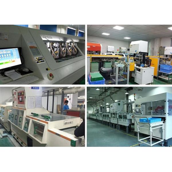
Workshop


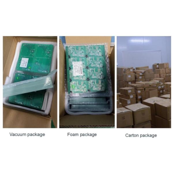
Common packaging
1.PCB: Vacuum packaging with carton box
2.PCBA: ESD packaging with carton box
FAQ
Q1.
What's your MOQ ?
No Moq ,We accept small orders as well as mass production.
Q2.
For small quantity orders, can you produce prototype PCB?
Haina lean Electronics Co., has the capability to produce circuit boards in any amount.
Q3.
Can You provide fast rotating PCB ?
Yes , we can provide fast service 24 hours .
Q4.
What are the services you can provide ?
One-stop contract manufacturing
PCB board, PCB Design & Layout, PCB Assembly, PCBA programming & functional testing, Electronic components purchasing service, Enclosure molding & final assembly with labels,instructions,enclosure, boxes.
Q5.
Whether all PCBA s will be tested before delivery ?
Yes , we will test each piece of PCBA product under your testing methods ,to ensure quality and functionality .
Q6.
Do you provide OEM service ?
Yes ,we offer PCB and PCBA OEM Service , we manufacture the PCB and PCBA products to your design and requirements .
Q7.
Shipping Cost ?
The shipping cost is determined by the destination ,weight ,packing size of the goods .We can provide shipping, air, land, express and other transportation services .
Q8.
Do you accept process materials supplied by clients?
Yes, we can provide component source, and we also accept component from client. OEM and ODM orders are accepted.
Company Brief Information
Haina lean Electronics Co., Ltd is a one-stop EMS supplier integrating PCB design, PCB manufacturing, Component sourcing and PCB assembly.
Here is strong component supply chain and procceurement team. Prototype and mass production are available.
Competitive price is for high-quality and services. Exported to worldwide customer in US, Europe, Canada etc.
Product Tags:

|
|
Double Side Fr1 Odm Lead Free Pcb Assembly 1/3oz Images
|


